
HDI PCB, comparing with standard build-up multiplayer PCB, achieves smaller size, higher connection and wire density with better electrical performance and signal precision in end products. HDI is currently widely used in mobile phones, digital cameras, MP3, MP4, laptops, IC carriers, automotive electronics, and others. HDI generally uses build-up manufacturing; more of layer count requires higher technical manufacturing capacity. Circuit Solutions now is capable of 1+N+1 and 2+N+2, with “copper filled” for special stacked holes, plating hole filling, direct laser drilling (DLD), laser direct imaging (LDI) and other advanced technologies.
Here are some advantages of HDI PCB:
The advantages of HDI PCB include:
• Reduce cost
• Increase connection and wire density
• Improve thermal performance
• Ameliorate RFI/EMI/ESD
• Increase design efficiency, electrical performance and signal precision
• Advance packaging techniques
General Specification of HDI PCB in Circuit Solutions:
Layer Count: 4-20Layers
Type of stack up: 1+N+1, 2+N+2
Material Available: FR4, High Tg FR4, Halogen Free FR4
Board thickness: 0.4-3.2mm
Finished copper thickness: 1/3oz – 3oz
Min. trace width/spacing: 3/3mil
Min. through hole: 0.2mm
Min. blind via: 0.1mm
Surface treatment: Immersion Gold, ENIG + OSP

-
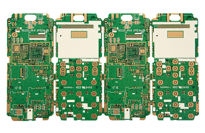
 HDI 3+N+3 Stack-up PCB
Layer count: 6 Layer
Board thickness: 1.4mm
Material: FR4
Min. Hole diametre: 0.4mm
Surface Treatment: ENIG
-
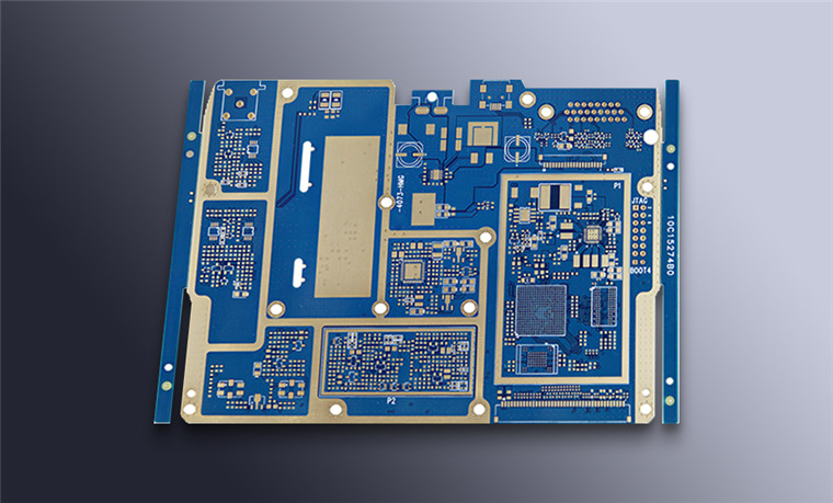
 HDI 3+N+3 Stack-up PCB/ Medical device PCB
Layer count: 3+6+3 Layer
Board thickness: 1.6mm
Material: FR4
Min. Hole diametre: 0.4mm
Surface Treatment: ENIG
-
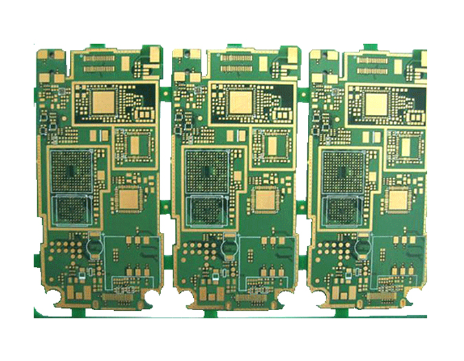
 HDI 3+N+3 Stack-up PCB
Layer count: 3+4+3 Layer
Board thickness: 1.6mm
Material: FR4
Min. hole diametre: 0.4mm
Surface Treatment: ENIG
-
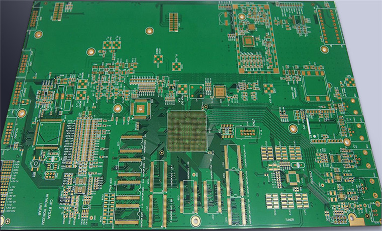
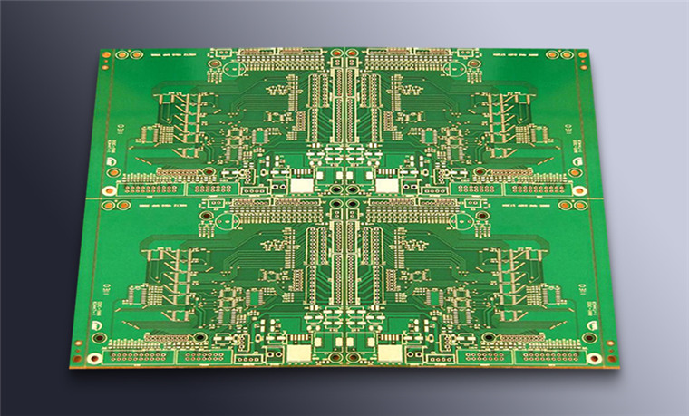
 Layer Count: 16 Layers
Type of stack up: 3+10+3
Material Available: FR4
Board thickness: 1.0mm
Surface Treatment: ENIG 1u"
-
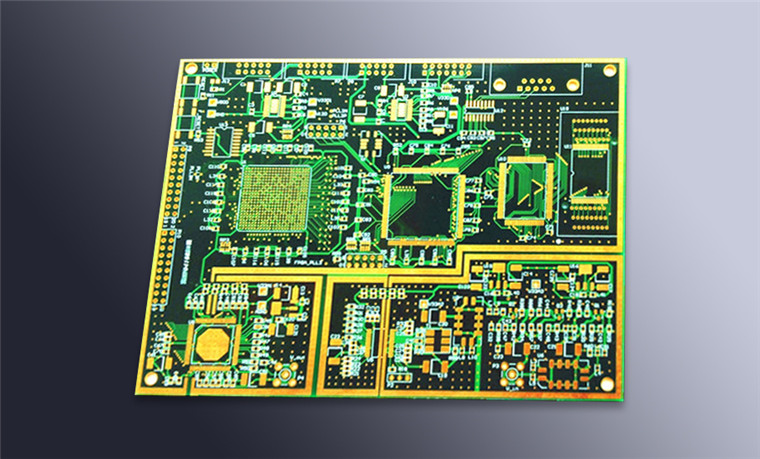
 Layer Count: 10 Layers
Type of stack up: 3+4+3
Material Available: FR4
Board thickness: 1.6mm
Surface Treatment: ENIG
-
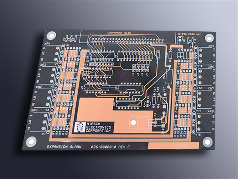
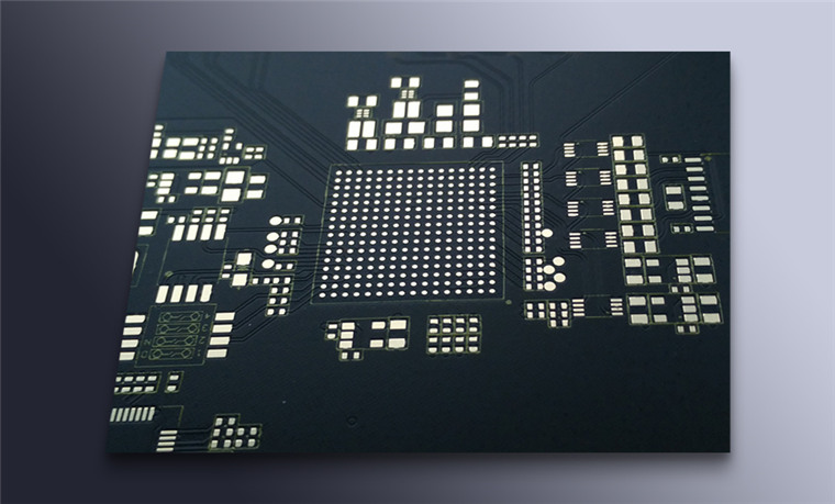 Layer Count: 4Layers
Type of stack up: 1+2+1
Material Available: High Tg FR4
Board thickness: 1.2mm
Finished copper thickness: 1oz
Min. trace width/spacing: 3/3mil
Min. through hole: 0.2mm
Surface treatment: ENIG
-
 Layer Count: 6 LayersType of stack up: 2+2+2Material Available: Halogen Free FR4Board thickness: 1.6mmFinished copper thickness: 1/3ozMin. trace width/spacing: 3/3milMin. through hole: 0.2mmSurface treatment: Immersion Gold
 -
 Layer Count: 4LayersType of stack up: 1+2+1Material Available: High Tg FR4Board thickness: 1.2mmFinished copper thickness: 1ozMin. trace width/spacing: 3/3milMin. through hole: 0.2mmSurface treatment: ENIG